Or, Reverse engineering a 6502 SBC
A few weeks ago I acquired a “IIeasy Print” automatic printer buffer/switch designed for Apple systems. It was a curiosity because it had a few nice features and appeared to be a self-contained system. The items below were discovered during research before the card arrived.
- CPU (believed to be a g65sc102 based on usenet posts, a cmos 6502 variant)
- 256k ram (two chips, 128kx8 PSRAM)
- 6 serial ports (6551 acia)
- system rom (unknown, believed to be 8k 2364 or 2764)
- system ram (6116 2kx8 sram)
The type of cpu and rom were unknown as they had stickers covering their information in any photos I could locate. Scouring the image of the card gave me the 6116 and 6551 chip ID’s, as well as a couple of others, such as 74ls138’s to assist address decoding and a 74ls374 near a 14 pin header.
Beyond this, the next step was to imagine possible memory maps and wait for the card to arrive.
Upon arrival, I eagerly opened the box and stripped labels off the unknown IC’s and identify chips further. The CPU was confirmed to be a g65sc102 CPU, and the master crystal was found to be 7.32mhz.
Regarding system speed, most 6551’s are set up with a 1.84mhz clock to get perfect data rates. The crystal is exactly four times the ideal clock. The 6551’s are gs65sc51p-2, indicating a 2mhz ceiling on system speed. As the CPU runs in sync with its IO chips, it’s also going to run at a max of 2mhz.
In effort to save costs, only one crystal is on card, and a system clock of less than 1mhz doesn’t sound reasonable for handling six serial ports, so a 1.8mhz system clock is assumed.
The next step is to verify the system’s memory map. As there’s a PLA on card, it’s not going to be easy to work out the memory map based on the PCB traces and logic on the card. Instead, I chose to brute-force the memory map via the CPU socket.
Before this could be configured I needed to decide on how exactly to scan the card for its memory map. The most straightforward method seemed to be driving the address bus through the CPU socket and monitoring the chip select signals on the individual IC’s. A relatively simple program could be built to do the work and create a log of what addresses involve each chip select line.

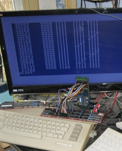
In the image above, you can see my trusty keyboard-enhanced Arduino work-alike. Most people would call this a Commodore 64, but in this case I’m using it in the way most people these days would use an Arduino.
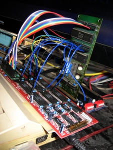
The vertical card is in a bus extender plugged directly into the Commodore’s memory bus. It’s loaded with a pair of R6522P VIA’s, each of which provide sixteen GPIO lines. The ribbon cables lead to an Atari VBXE adapter. The adapter simply mirrors the 40 pins in the dip socket to a header on the side, making it easier to connect to the socket reliably. Due to physical constraints, I had to insert the adapter upside down, but it can still serve its purpose in this configuration.
The upper VIA has all sixteen GPIO lines routed directly to the CPU socket’s address pins. You can see this configuration with the two 8-line ‘rainbow’ cables leading from the vertical card to the IIeasy Print card under test.
The lower VIA serves two purposes: First, port B’s higher bits control the CPU socket’s control bus, managing /reset, r/w, and phi2. This is the smaller ribbon cable that has blue, white, grey, and purple connecting to the left edge of the header on the CPU socket.
The lower bits on port B as well as all bits on port A are configured as inputs, monitoring chip select signals on each IC I believed to be a memory bus target: The 2k SRAM, each of the 128K sram’s, the system rom, the six 6551 ICs, and the 74ls374. For socketed ICs, I simply lifted them from their sockets and attached a male pin lead to the /cs line on the target. /OE was ignored as most systems based on the 6502 will ground /OE and use /CS and /WE to control the IC. Chips without sockets had a test pin tack-soldered to their respective /CS (or CLK line in the 74ls374’s case) and a male-female pin lead was routed to the lower VIA’s port A lines.
The next step is to write a program to scan the card. I wrote this in BASIC. BASIC is slow, but it’s built into the system ROM on the Commodore and does its job well.
10 V0=56864
11 V1=56880
12 PB(0)=V0
13 PA(0)=V0+15
14 PB(1)=V1
15 PA(1)=V1+15
16 POKE V0+2,255:POKEV0+3,255:REM OUT
17 POKE V1+2,240:POKEV1+3,0
18 REM VIA 0A:     ADR LOW
19 REM VIA 0B:     ADR HIGH
20 REM VIA 1A:     CHIPSEL READBACKS
21 REM VIA 1B7:    PHI2 OUT
22 REM VIA 1B6:    R/W OUT
23 REM VIA 1B5:    RESET OUT
24 REM VIA 1B4:    UNASSIGNED
25 REM VIA 1B3-0: CHIPSEL READBACKS
50 PRINT "{clr}RESETTING BOARD"
60 POKE PB(0),0:POKE PA(0),0
70 POKE PB(1),0:FORT=1TO300:NEXT
80 POKE PB(1),32
90 PRINT"DONE.  SCANNING.{down}"
100 FOR AH=0TO255
110 POKE PB(0),AH
120 FOR AL=0TO255
130 POKE PA(0),AL
140 PRINTAH*256+AL"{up}"
150 Y=PEEK(PA(1))
160 X=PEEK(PB(1))
170 IF X<>OX OR Y<>OY THEN GOSUB 200
190 OX=X:OY=Y:NEXT:NEXT:END
200 REM PRINT REPORT
210 PRINT ,"NEW: ";
220 B=(X AND 15)
230 GOSUB 300
240 B=Y
250 GOSUB 300
260 PRINT
270 RETURN
300 REM PRINT BIT PATTERN
310 FOR T=7 TO 0 STEP -1
320 PRINTMID$(STR$(SGN(BAND(2^T))),2,1);
330 IF T=4 THEN PRINT" ";
340 NEXT
350 PRINT"  ";
360 RETURN
Initial testing confirmed my bus scanner was working correctly by manually setting GPIO lines and checking the 2k SRAM’s /cs pin. As expected, the 2k SRAM turned out to be at address 0, so it made a good test target.
From there, the program was run and left to scan the bus, while it displayed any changes in the chip select lines’ outputs.
After the program was run, I evaluated the chip select log and came to this memory map as a conclusion:
Address Range IC Desc
0000-07ff U503 2116 soldered-in ram
0800-1fff U503 mirrors of U503
2000-9fff u401/2 Buffer ram (256k is bankswitched here)
a000-bfff empty
c000-c01f U101 6551 acia
c020-c03f U102 6551 acia
c040-c05f U103 6551 acia
c060-c07f U104 6551 acia
c080-c09f U105 6551 acia
c0a0-c0bf U106 6551 acia
c0c0-c0df U701 74ls374
c0e0-c0ff unknown
c100-c7ff Mirrors
c800-cbff U504 Read jumpers
cc00-cfff Buffer RAM mapping
e000-ffff U502 Firmware ROM (2764)
Of interest to me was that only 7 of 8 devices are present in the C000 range, and that only 32k of the 128k memory was mapped. It’s time to read the ROM and get some more educated guesses about the card.
Since most of the hardware to fully control the card was already set up, I placed the system ROM back in its socket and changed the lower VIA’s port A to attach to the data lines. I slowly but surely extracted the system code from the card and saved it to a file.
After loading the data into RAM on the Commodore and viewing it in a debugger, there appeared to be an initial store that wasn’t obvious: The CMOS ‘STZ’ instruction was used to store a 0 into $CC00, and the debugger didn’t understand CMOS opcodes. Further testing and experimentation discovered that the $CC00 register controls memory banking on the two 128k SRAMs as detailed below:
Bit Effect
0 A15 on U401 and U402
1 0=select U401, 1=Select U402
2 A16 on U401 and U402
There are also many writes to the $C0E0 location in memory, but I wasn’t able to determine what IC is connected to it. I might discover that later.
As I’m now aware of the system’s memory map, I could consider other uses for the card. Currently, I”m working on a port of the original Apple2 System Monitor, as it’s almost as simple as a system firmware can get, requires only 2k of space, and is something I’m quite familiar with. In ideal conditions the only real work for getting minimal functionality from the system monitor firmware would be patching code that writes to the screen and reads from the keyboard. From there, additional changes could be made. That will be covered in a later post.
Edited May 14 2015 to correct the ACIAs’ addresses.


Pingback: Examining Vintage Printer Server Hardward for Apple II
Pingback: Examining Vintage Printer Server Hardward for Apple II | Hack The Planet
Wow!
That’s an excellent job of reverse engineering for that gizmo.
Thanks Gregg 🙂
You are very welcome. Continue the good work with your efforts.
Keep an eye on me over the next few weeks, I’ll be trying to get a debugger of some sort running on the card. 🙂
Pingback: Examining Vintage Printer Server Hardward for Apple II | Maker of Meta
Very interesting read. Nice to see the BASIC code as well. (Except, I’ll have to stare at it for much longer to make sense of how it works.)
Thanks. 🙂 It’ll help if you have the 6522 VIA datasheet on hand while reading the program. Google will be your friend there, as there’s still a company making a pin compatible IC.
Pingback: Commodore C64 printer buffer | Commodore Is Awesome